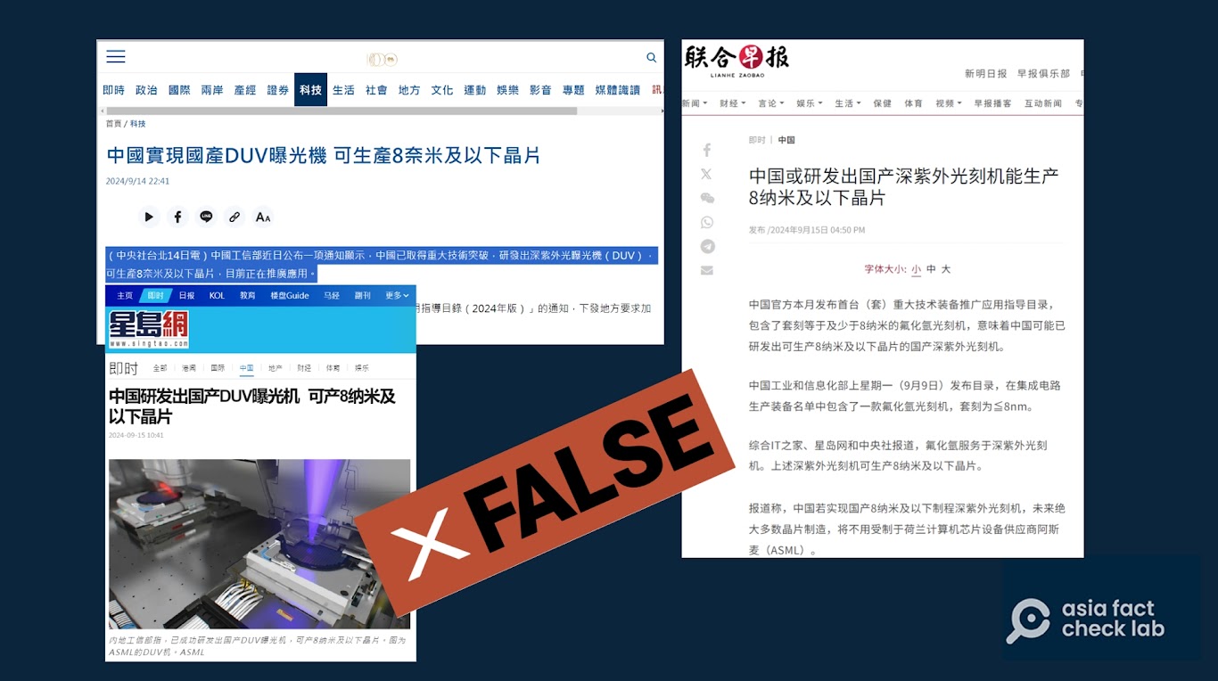
China's Ministry of Industry and Information Technology (MIIT) released an industrial document on September 2, mentioning that Chinese manufacturers had successfully produced a lithography machine (exposure machine) with a "register accuracy" of less than 8 nanometers. Subsequently, some media reports interpreted China's photolithography machine as "capable of manufacturing chips of 8 nanometers and below", triggering a wave of domestic fervor about the semiconductor industry's full technological autonomy and its success in realizing the bend in the road to overtake the car.
However, based on my understanding of China's chip industry, I don't expect much from this kind of news, as I know that this kind of technological breakthrough is still far from the level created by the publicity. However, when discussing this topic with my wife, I found it difficult to explain it clearly, so I spent some time today checking this out.
First of all, to understand what this "8nm" really means, we have to figure out what the "nesting accuracy" is.
The term "nesting accuracy" refers to the precision of the alignment between the different layers of a chip when it is being manufactured. As an analogy, when building a tall building, each floor needs to be perfectly aligned, otherwise the building will be crooked. The so-called 8-nanometer "set engraving accuracy" means that the lithography machine in the different layers of the alignment between the accuracy of 8 nanometers. But this is only in the alignment level performance, and we usually say 8 nm process node is not a concept.
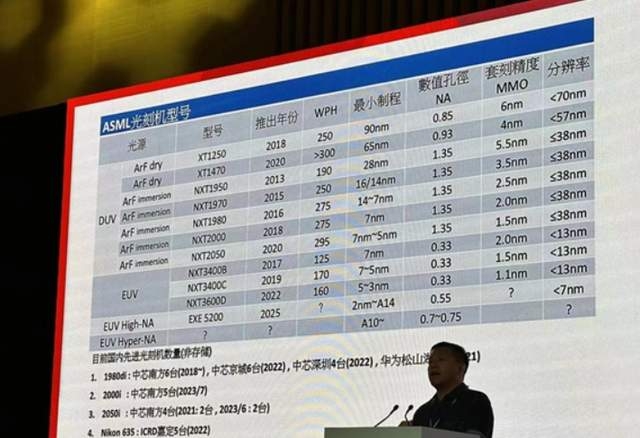
So what kind of chips can this lithography machine make compared to Asmax? According to the information, the resolution of this Chinese lithography machine is 65 nanometers, which means it can only produce chips of 28 nanometers or larger process, and there is still a big gap from the world's most advanced 7-nanometer chips.
By the way, here's why a lithography machine with a resolution of 65 nanometers is still capable of making a 28-nanometer chip. To answer this question, we first need to understand a little about the basic process of chip manufacturing.
Analogously, the chip-making process is like the projection of a movie film; simply put, each layer projected corresponds to a layer of the chip. In this part of the process, China's domestic photolithography machine can only produce 65-nanometer chips. However, through certain technical means, it is possible for this lithography machine to achieve a precision of 28 nanometers.
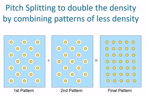
The technique of multiple exposure means that the same area needs to be exposed multiple times to make the circuit lines of the chip smaller and more precise. Continuing with the movie film analogy, imagine having two projectors projecting onto the same screen at the same time, doesn't the image on the screen become much more complex all of a sudden?
The key to multiple exposure technology in this process is "registration accuracy". It ensures that the images are precisely aligned each time they are projected, resulting in greater manufacturing precision. It is here that the value of register accuracy is fully realized.
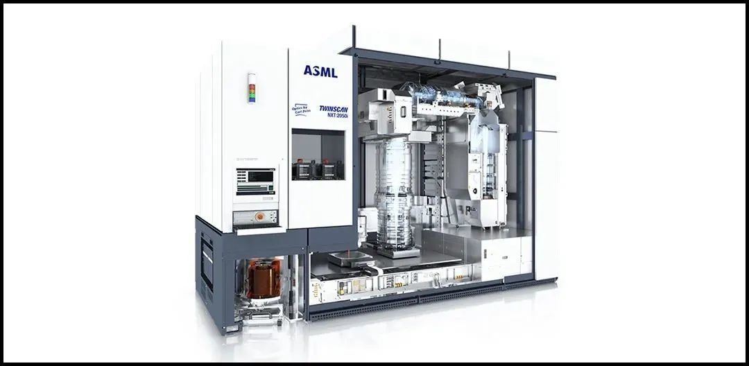
Speaking of which, we have to mention Huawei's 7nm domestic chip for its cell phones. How did we make a 7-nanometer chip without having a 7-nanometer lithography? Behind this relies on the veryMulti-exposure technology. However, it's certainly not using the same photolithography machine mentioned earlier, but a much higher precision device, an advanced photolithography machine from Asmax.
So how did China produce the 7nm chip in the previously released cell phone in spite of the foreign technology blockade? Using advanced DUV lithography (deep ultraviolet lithography). Theoretically, it is possible to realize a 7-nanometer process:
Specifically, they break through the limitations through the following two techniques:
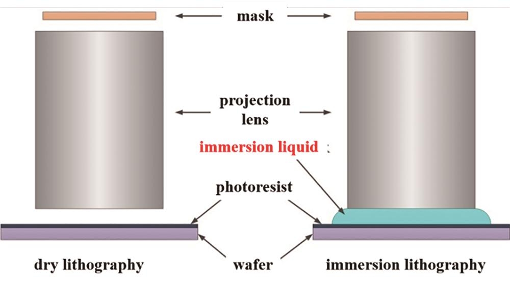
The first is immersion lithography: by adding a layer of water between the light beam and the chip, the light is made "thinner" so that smaller circuits can be etched. Simply put, this shortens the wavelength of the light by refracting it through the water, allowing the DUV lithography machine to achieve a higher level of resolution. Why would adding a layer of water make the DUV's light "thinner" and thus smaller? Don't understand? Look in your physics book. It's called refraction, and the refracted light has a shorter wavelength, so follow the axioms and memorize them.
The second item is the multiple exposure we described earlier: that is, the same place needs to be exposed several times in order to make the chip's circuitry more precise and detailed.
While it is barely possible to produce 7-nanometer chips by these technological means, it brings with it some obvious drawbacks:
-It's very inefficient.: This method takes more time and is very slow to produce.
-Extremely high cost: Producing chips in this way is very expensive and not economically viable.
-Low yield rate: that is, many of the chips produced may not meet the standard of perfection.
Therefore, this high-cost and inefficient mode of production will only be chosen if other strategic or political factors are taken into account in addition to economic benefits.
The final problem is that China's lithography is on a different development path from the world's most advanced lithography. It is just like the same operation, others hold a scalpel, we hold a kitchen knife in our hands.
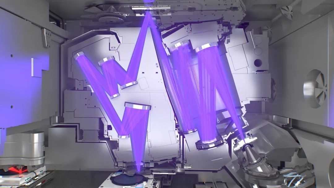
We have developedDUV lithographyUsing theDeep ultraviolet light, which has light wavelengths of193 nanometers. It's okay to do some simple surgeries with this chopper, but if you're doing delicate surgeries like heart or brain, you have to use a scalpel. Currently the world's most advanced lithography using EUV lithography (extreme ultraviolet lithography), the light source wavelength of only13.5 nmIt's like a handful. It's like a handful ofultra-sharpThe carving knife, which is capable of carving directly7nm, 5nm, even smaller chips. This not only means that it can create more sophisticated and efficient chips, but also faster and cheaper to produce.
Facing the gap and learning from the ground is the scientific attitude. This is where the gap lies between Chinese lithography and the most advanced international equipment.
